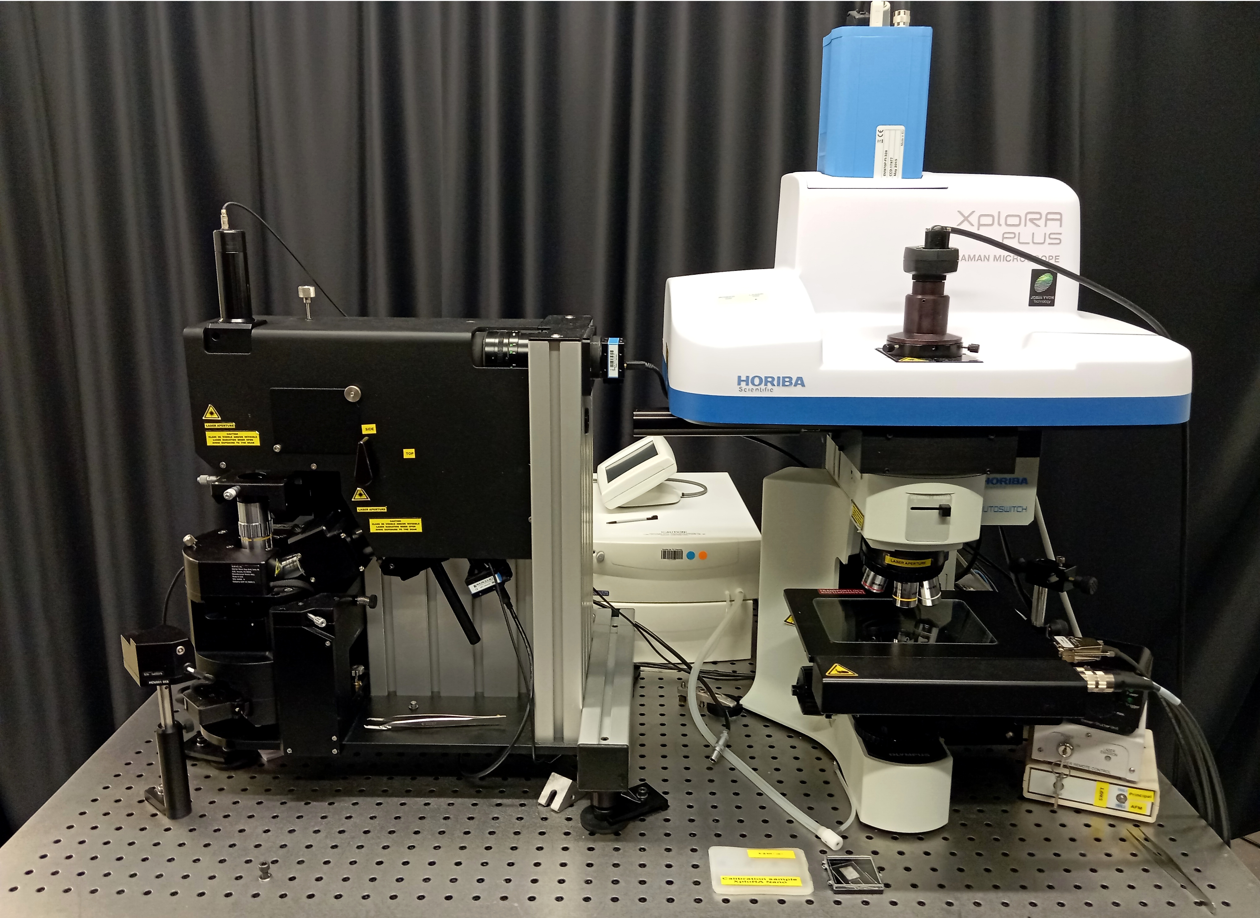
Horiba XploRA
Contact:
Application |
|---|
|
Specifications |
|---|
|
Contact:
Application |
|---|
|
Specifications |
|---|
|

TU Chemnitz Completes Collaborative Project Funded by the German Academic Exchange Service with ENET'COM and Industrial Partner Dräxlmaier Group …

Call for participation in a short linguistic survey by Chemnitz University of Technology – no specialist knowledge needed …
Visiting Scholar Benanchour Saidi at the Junior Professorship of Intercultural Practice with a Focus on Digital Cultures …
Chemnitz University of Technology researchers uncover a new way to amplify light-matter coupling in graphene using tin nanoantennas, published in “Advanced Optical Materials” …
The study analyzes 2D MoS₂ nanoflakes and twisted bilayers. It shows …
Semester and internship abroad worldwide! Learn about partner universities, funding opportunities …
Which course of study suits me? Which requirements do I have to fulfill? What can I experience in …