Technical Equipment
Please don't hesitate to contact us in the case you feel, that your problem could be solved using our methods and our equipment..
Scanning Probe Microscopy
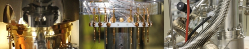
Low Temperature STM
- Scanning tunnelling microscopy/spectroscopy at low temperature of down to 4.5 K
- In situ epitaxial growth of molecular adlayers
- Electrospray system for bulk and fragile molecules deposition
- Low energy electron diffraction (LEED) measurements
- Sputter anneal cycles of metal crystals

Variable Temperature STM
- In situ epitaxial growth of molecular adlayers
- Low temperature scanning tunnelling microscopy with flowing cryostat
- Low energy electron diffraction (LEED) measurements
- Sputter anneal cycles of metal crystals


Burleigh ambient STM
- Ambient STM
- Electronic controller system from Burleigh Instructional STM
- Atomic Force Microscope (Burleigh)
- Scanning Electrical Force Microscope (SEFM) (Extension of TopoMetrix AFM)

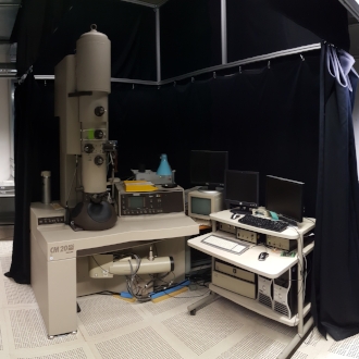
Electron Microscopy
Philips CM 20 - currently not operational
- 200 kV High Resolution Transmission Electron Microscope
- Field Emission Gun (FEG)
- Gatan Imaging Energy Filter (GIF)
FEI Nova NanoSEM 200
- Schottky Field Emission Gun
- Backscattered Electrons
- Analytical Detectors for:
- X-ray Microanalysis
- Electron Backscattering Diffraction (EBSD)
- Cathodolumineszenz

Spectroscopy
EELS - LEED
- EELS-LEED: Electron Energy Loss Spectroscopy - Low Energy Electron Diffraction
- Equipped with a deflection unit, enables precise control over momentum transfer
- High energy resolution is achieved
- 0.01 invAngstrom momentum and 10 meV energy resolution
- Measure low energy excitations (i.e., plasmons)
- Unique homemade tool

Diffraction
SPA - LEED
- SPA-LEED: Spot Profile Analysis - Low Energy Electron Diffraction
- A unique tool, originally developed in Hannover by M. Henzler
- Two geometries in reciprocal space: normal geometry of incidence and grazing geometry of incidence
- Low-resolution scanning electron microscopy mode
- CEM (channeltron electron multiplier) analyzes the reflected intensity and enables recording spot profiles

Transport
4pp-STM/SEM
- Transport experiments down to nanoscale
- Four individually controlled STM-tips
- High resolution SEM for observation and e-beam lithography
- Flow cryostate for a wide temperature range
- In situ epitaxial layer growth and characterization by LEED

Magnetotransport
- Electronic transport in low-dimensional nanostructures in dependence of a magnetic field from -4 to +4 T
- The angle between the magnetic field and the sample is freely adjustable
- Temperature dependent transport from 10 to 400 K
- In situ growth of epitaxial thin films
- Low energy electron diffraction (LEED) measurements
Mechanically Controllable Break Junction
MCBJ
- Contacting of single molecules
- Cooling possibility down to 70K
- Stable atomic point contacts up to 1 hour
Light Microscopy
Keyence Digital Microscope VHX-500
- Transmitted- and reflectet-light operation
- Different objectiv lenses
- Camera resolution 1600x1200 px

Preparation
Ion Beam Milling System
Leica TIC020
- Triple Ion Beam Milling System
- Allows target preparation of samples for SEM analysis
- Suitable for cross-section preparation of any material with little pre-preparation required
- Different voltages and currents available
- Time controlled

Ion Beam Milling System
Leica TIC 3X
- Triple Ion Beam Milling System
- sample cross-sections and flat surfaces to be produced for SEM, EBSD and AFM examinations
- Prepreparations may be required before use
- Different voltages and currents available
- Time controlled

Ion Milling System
Leica RES 102
- Sample thinning and polishing
- Different voltages and currents available
- Time controlled

Mechanical Sample Processing
Leica TXP
- Device for sample preparation
- For cutting, milling, sawing, grinding, polishing samples before use / processing in TIC 3X or TIC 020