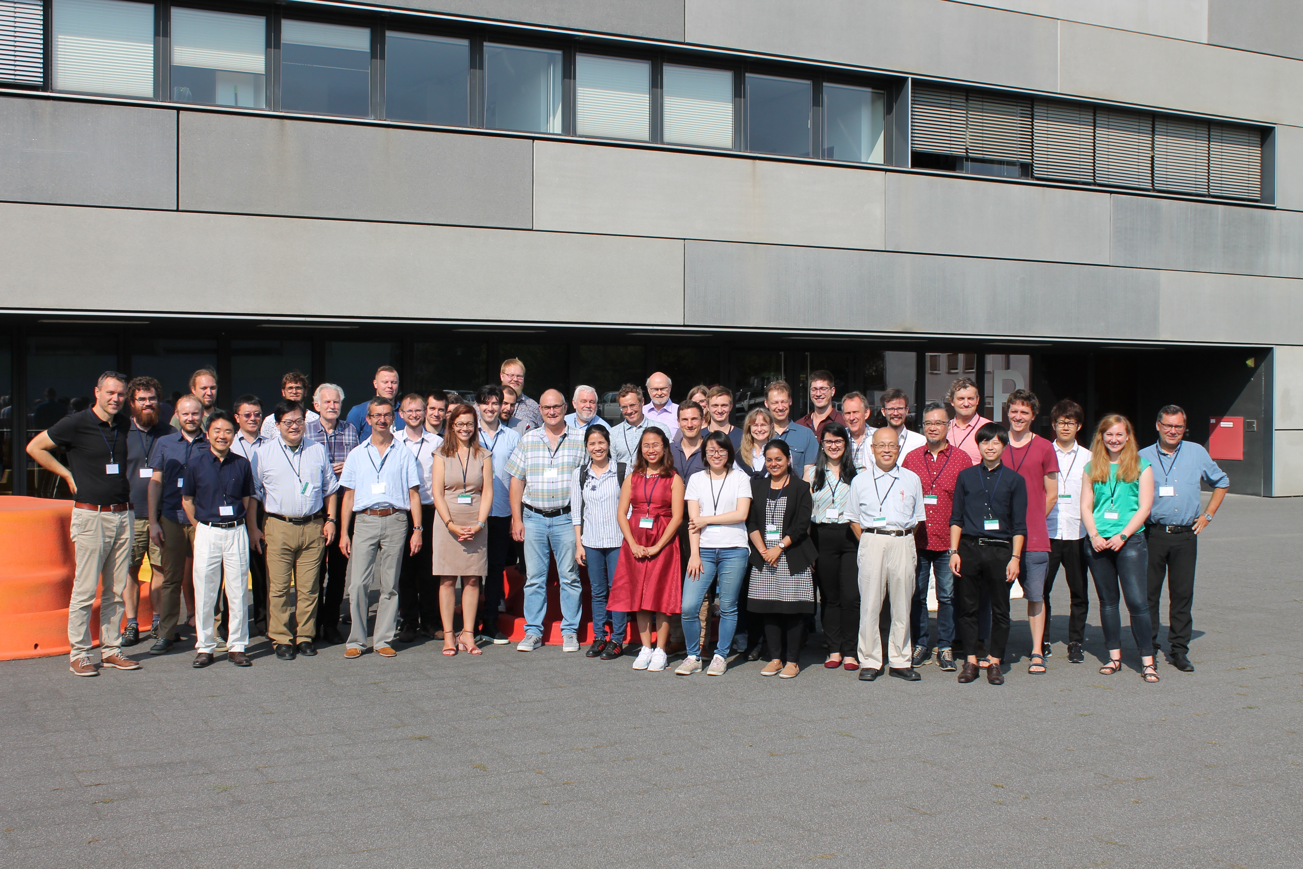
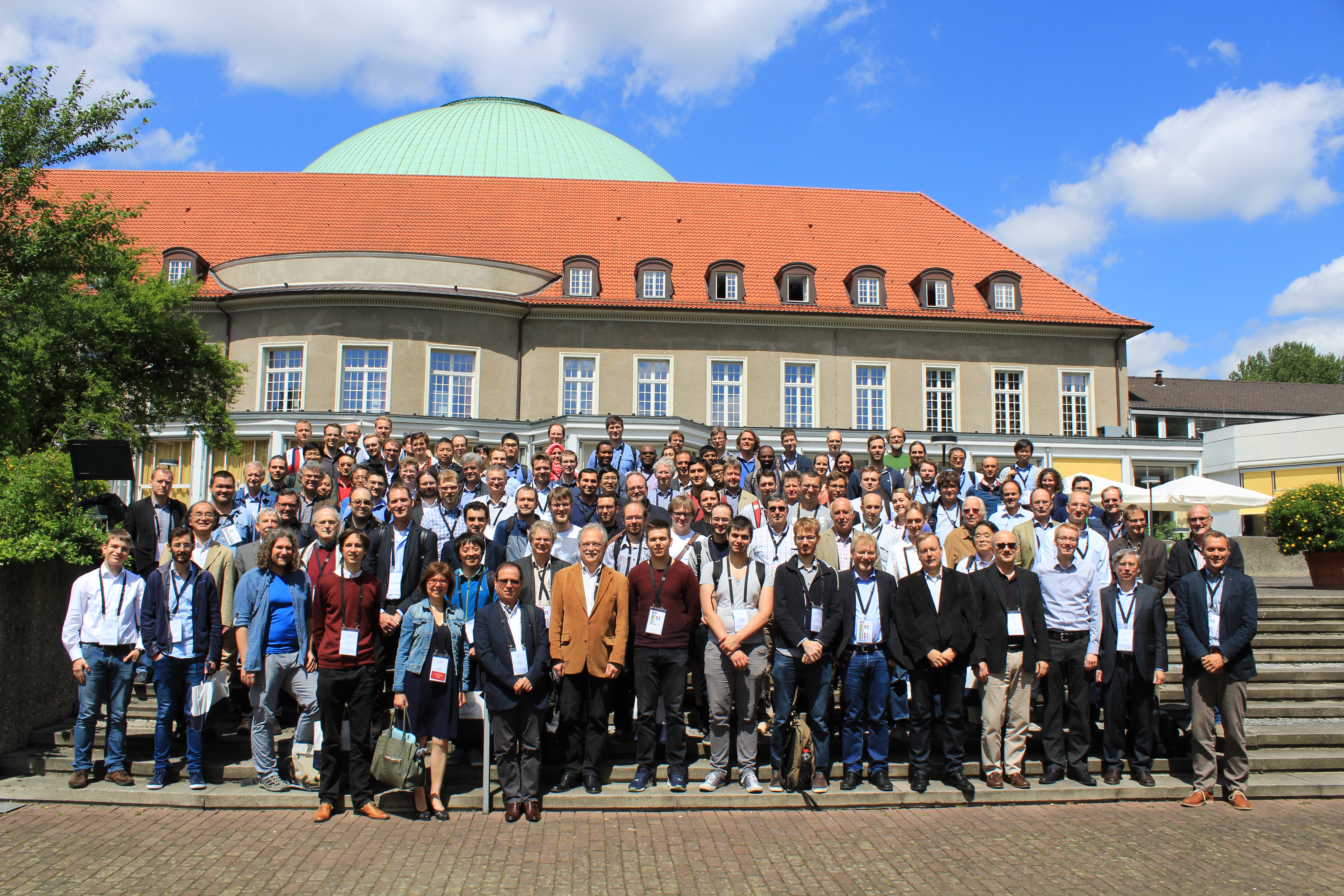
Workshops & Symposia
6-7 June 2024, PTB Braunschweig
From June 6-7, 2024 we held our 2nd workshop with all members of FOR5242 at the PTB in Braunschweig

21-22 March 2024, Berlin
During the DPG Spring meeting 2024 in Berlin we organized from our DFG Research Unit FOR5242 a focus session on "Proximity Effects in Epitaxial Graphene". Invited speakers were Klaus Ensslin (ETH Zurich), Kathrin Küster (MPI Stuttgart), Stephen Power (Dublin City Univ.) and Jose Lado (Aalto Univ.)

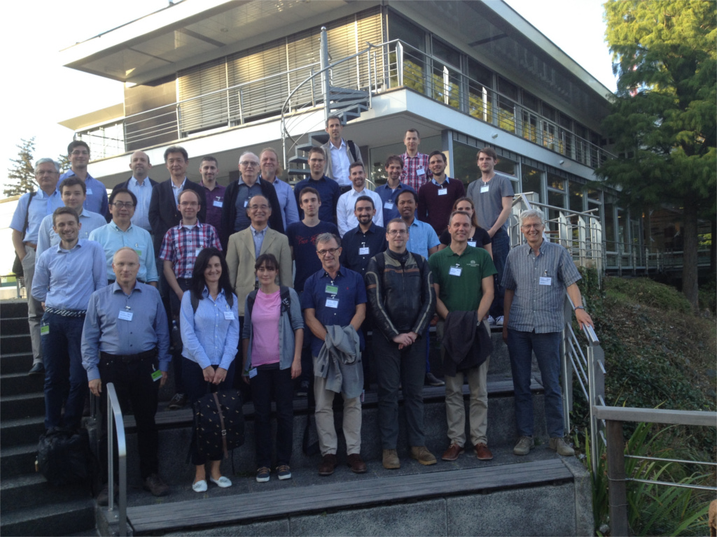
11.-15. September 2023, Karlingerhof, Österreich
From 11-15 February 2023 the first retreat meeting of our workshop with all members of the research group FOR5242 took place in Achensee, Austria.

10.-13. September 2023, ETH Zurich, Swiss
Details are available at AOFKA 2023.
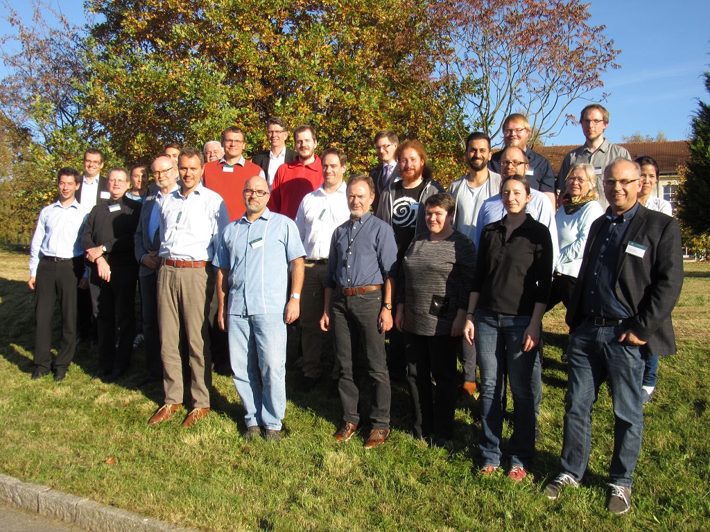
2 - 3 February 2023 in Göttingen, Germany
From From 2-3 February 2023 our workshop with all members of the research group FOR5242 took place in Göttingen. In numerous talks and by means of posters, recent results on proximity induced effects in 2D graphs were presented. The scientific program can be found here

6 - 8 October 2021 in Freiberg, Germany
The international AOFKA21 conference was held from 6th to 8th of October 2021 at the TU Freiberg, Germany.

25 - 28 August 2019 in Chemnitz, Germany
The 2019 International Symposium on Epi-Graphene was held from 25th to 28th of August 2019 at TU Chemnitz, Germany. The meeting was devoted to the science and application of epi-graphene on silicon carbide. Aspects of growth, characterization, functionalization by, e.g. intercalation and applications are discussed from experimental and theoretical point of view.
Schloss Ringberg, 17- 20 February 2019
At the conference center of the Max-Planck Society, Schloss Ringberg, was a 3-day symposium on correlated and collective phenomena in low dimensional structures and complex materials. Confirmed keynote speakers were: Silke Biermann (Paris), Ralph Claessen (Würzburg), Hanno Weitering (Tennesee), Franz Himpsel (Madison), Michael Horn-von Hoegen (Duisburg-Essen) and Uli Höfer (Marburg). More details can be found here. The symposium was organized by the Research Unit FOR1700 and the FHI in Berlin.

TU Chemnitz, 24 January 2019
A central part of this meeting was a mutual exchange on current issues and methods related to transmission electron microscopy. The status of the application for the new TEM center was also a subject.
Forschungszentrum Jülich, 19- 21 September 2018
This workshop aimed to bring together the experts in the field of 4-tip STM surface transport measurements, as well as researchers interested in this new technique. The participants presented their latest results on nanoscale charge transport, obtained with multi-tip techniques. Also, common experimental issues and aspects of the data analysis which occur for this new technique were discussed during the workshop.
TU Chemnitz, 19. Oktober 2017
Bei diesem Workshop wurden in fakultätsübergreifender Weise die laufenden TEM-Aktivitäten der TUC kurz vorgestellt. Ziel war es einen Überblick über die TEM Aktivitäten zu bekommen.
Hannover Congress Centrum, July 02 - 07, 2017
The 16th International Conference on the Formation of Semiconductor Interfaces (ICFSI-16) was hosted in Hannover, Germany. ICFSI-16 was primarily focused on phenomena at surfaces, interfaces, and nanostructures that are of strong current interest, based on semiconductor or insulator surfaces and interfaces, ranging from characterization at the atomic scale to prospects of applications.
Further Information can be found here.
Desden, March 21, 2017
Complex nanostructures on surfaces, e.g graphene nanoribbons, nanorods, atomic wires, or molecules in between junctions, provide a perfect platform to study both fundamental and application driven aspects. Many properties such as a targeted functionality of the nanostructure, instabilities, phase changes, etc. can be addressed and smartly probed by electron transport. 4-tip scanning probe techniques became very popular within the last years and have demonstrated their capability to address important physical and chemical aspects.
Further Information can be found here.
Bad Honnef, March 1–3, 2017
The "round-table", organized by research units FOM-1D, FOR1162 and FOR1700, covered hot topics of low dimensional physics, e.g. magnetism at the atomic scale, superconductivity in 2D, topologocally protected edge states, spin-orbit coupling, etc. Experimental realizations at surfaces were presented as well as state of the art theoretical descriptions of these high correlated systems under explicit consideration of the environment.
Follow this link to download the program.
Workshop at the Research Center Jülich, September 21-23, 2016
This workshop aimed to bring together the experts in the field of 4-tip STM surface transport measurements, as well as researchers interested in this new technique. The participants presented their latest results on nanoscale charge transport, obtained with multi-tip techniques. Also, common experimental issues and aspects of the data analysis which occur for this new technique was discussed in a technical session.
Further information can be found here.
Hannover, May 28-29, 2015
The workshop focused on recent advances in controlling and characterizing of films and surfaces, with a particular emphasis on materials for energy, electronic, and spintronic applications.
Further information can be found here.
Schloss Herrenhausen Hannover, April 7-10, 2015
This Symposium aimed to bring together leading scientists from different disciplines to examine the potential of this rather unexplored field of research.
Further information can be found here.
DPG Frühjahrstagung Dresden, March 31 - April 4, 2014
The Sections of Surface Science, Semiconductor, Thin Films and Low Temperature of the DPG organized a Joint Symposium about "One-dimensional Metals: Reality of Fiction".
Further information can be found here.
FKA17 Chemnitz, July 1-3, 2013
The central aim was the exchange of ideas between analysts, materials scientists, solid state physicists and technologists.
Further information can be found here.
Bad Honnef, Februrary 13-15, 2013
Further information can be found here.
FKA15 Chemnitz, July 12-16, 2009
Further information can be found here.
DPG Frühjahrstagung Berlin, Februrary 25-29, 2008
Further information can be found here.