
Nanosciene on the atomic scale: new quantum materials
Our research comprises experimental studies on complex nanostrcutures, e.g. thin films, emergent 2D materials, 1D metallic systems and organic hybrids. Thereby, the growth and manipualtion of complex and robust quantum systems and quantum materials is the focus of our research. A comprehensive characterization regarding atomic structure, electronic states and electronic transport properties is maintained by using electron microscopes and scanning tunneling microscopy-based techniques.
Manipulation of the electronic properties of graphene
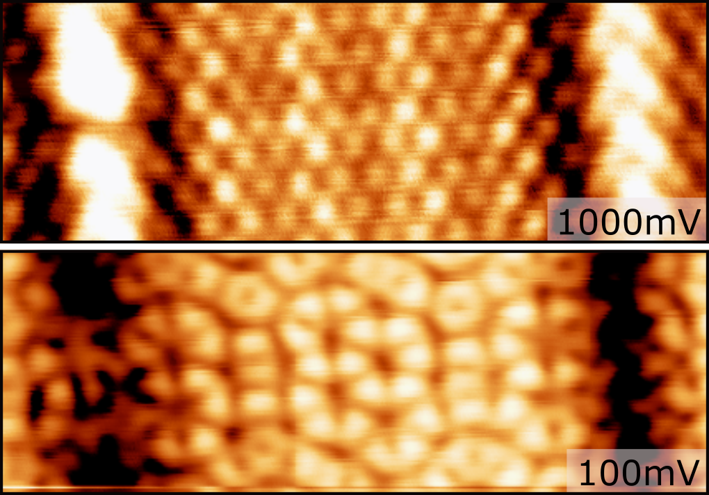 Epitaxial graphene on SiC(0001) is usually fabricated by heating the substrate. First, a carbon layer with a (6√3x6√3)R30° structure is formed on the surface, which is referred to as the buffer layer. One-third of the atoms in this layer are covalently bonded to silicon atoms in the topmost substrate layer, resulting in a buckling of the layer with a (6x6) structure. Further heating produces a second layer of carbon, which now acts as the buffer layer, and the first layer is transformed into a graphene layer with a delocalized π-electron system.
A conversion of the buffer layer into a graphene layer while avoiding the formation of a new buffer layer is possible through the intercalation of another element. This was first shown for hydrogen. The covalent bonds to the substrate are broken and saturated by H atoms, resulting in a quasi-free-standing graphene layer.
Our research within the research group FOR-5242 concentrates on the intercalation of heavy elements such as Pb, Bi or Sn in order to use the proximity effect to modify the electronic properties of graphene and thereby make it suitable for long-term applications, e.g. in electronics or in spintronics. The systems are characterized using electronic transport (four-tip STM/SEM, magnetotransport) and scanning tunneling microscopy (low-temperature STM).
Some relevant publications:
- Surface Transport Properties of Pb-Intercalated Graphene
- Comeback of epitaxial graphene for electronics: large-area growth of bilayer-free graphene on SiC, 2D Materials
Molecule/nanostructure hybrids
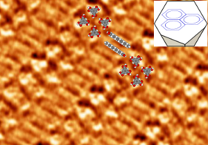 The utilization of molecules as functional elements in logic circuits is crucial for the realization of molecular nanoelectronics. In our group, we therefore deal with chemical aspects and surface reactions in order to create molecular networks with new properties. Using tunneling microscopy and spectroscopy (ambient STM RHK 300, low-temperature STM), the structural and electronic parameters are imaged at the atomic level. In particular, we are currently investigating polyalanine molecules which, due to their chirality, have a spin-selective effect on the conduction electrons (see also chiral induced spin-selectivity (CISS) effect), and are therefore suitable for application in spintronics.
Some relevant publications:
- Heterochiral Dimer Formation of α-l- and α-d-Polyalanine Molecules on Surfaces
- Charge-Ordered α-Helical Polypeptide Monolayers on Au(111)
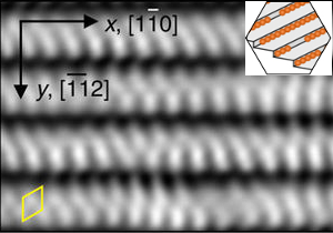 The electronic properties of low-dimensional systems are closely related to their geometric structure. The confinement of the charge carriers is of central importance in one-dimensional (1D) and two-dimensional (2D) structures, which can lead to electronic correlation effects and thus to deviations from the Fermi liquid behavior. These phases compete with partly intrinsic instabilities (phase transitions) or even show new quantum states due to spin-orbit coupling.
Ultimately, the smallest 1D structures can be realized, for example, by self-organization of monolayer and submonolayer structures of different atoms on (vicinal) semiconducting substrates, e.g. Pb/Si(557) or Au/Si(553), and have been discussed in our research group FOR-1700, among others. Furthermore, metallic 1D edge channels also occur in bismuth islands on graphene and Pb-intercalated graphene, which we are investigating in the research group FOR-5242.
Some relevant publications:
- Exceptional ballistic transport in epitaxial graphene nanoribbons
- Observation of correlated spin–orbit order in a strongly anisotropic quantum wire system
 Thin films are building blocks for modern material-based research and applications (lightweight constructions, data storage, etc.). For instance, the possibility of co-deposition and tunable growth on various substrates allows to fabricate condensed matter phases with new physical bulk properties but also defined interface and surface structures.
Therefore, we look in detail for defects (grain boundaries, chemical composition) as well as surface and interface structures. Besides TiNa alloys, epitaxial Bi(111) films and topologically non-trivial BiSb(111) films on Si(111) are currently investigated. For the latter the confinement and interaction of the bulk bands with the spin-polarized surface states are currently of interest.
Some relevant publications:
- Magnetoconductance in epitaxial bismuth quantum films: Beyond weak (anti)localization
- Surface state conductivity in epitaxially grown Bi1−xSbx(111) films
- Scattering of charge carriers by Cr impurities in magnetotransport on a Bi(111) ultra-thin