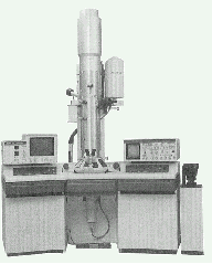
Transmission electron microscope HITACHI H8100 (200 kV, LaB6 cathode, with scanning unit for transmission and surface imaging) with fine-range electron diffraction (SAED) and X-ray micro-range analysis (EDXS / GENESIS)
-
Examination of thinned sample areas (residual thickness 30 - 300 nm) in cross-section or plane section of:
- Materials, composites and composite materials
- Coatings
- Magnification range: 1,000x to 200,000x
-
Statements on:
- Crystallite size, shape, orientation,
- Lattice defects, phase identification,
- State of inner boundary surfaces
- Spatial resolution of fine-range electron diffraction: approx. 500 nm
- Spatial resolution of the X-ray micro-range analysis: approx. 50 nm
Research methodology (pdf-file - 770kb)