Career launch during the ‘Open Day’
Since December 2014, Dr. Danny Reuter holds the Department of Lithography and Pattering Processes at the Centre for Microtechnologies – the Open Day brought him once again to Chemnitz
-
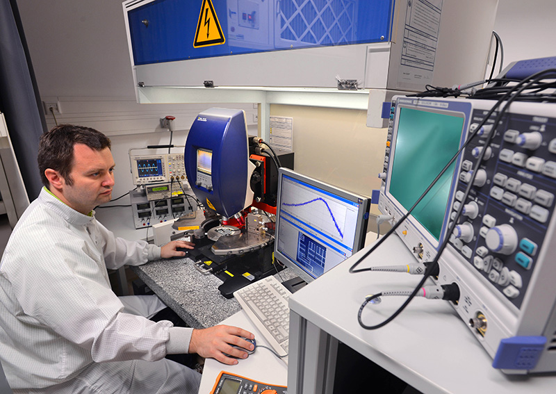
Dr. Danny Reuter characterizes AIM acceleration sensors of the Laser-Doppler vibrometer. Photo: Wolfgang Thieme
When Danny Reuter returned to his native city of Chemnitz in the spring of 1996, he had no idea that it is going to be his new home. The high school graduate from Schleswig-Holstein was in search of a place to study at that time. During the Open Day of TU Chemnitz, he has informed himself about the local offers. Ultimately, he was convinced by Prof. Dr. Wolfram Dötzel’s lecture to start his Electrical Engineering degree in Chemnitz, which he successfully completed in 2002. Subsequently, Reuter received an offer from Prof. Dr. Thomas Geßner for a PhD position at the Centre for Microtechnologies. The decision was not a difficult one: “The professor enjoys a high reputation among students and has many contacts in the industry. I therefore seized the opportunity and did my doctorate there.“ Thematically, he was concerned with thin-film encapsulation of acceleration sensors that are to be found in any car or mobile phone. Subsequently, the newly crowned doctor joined Fraunhofer Institute for Electronic Nano Systems ENAS, which works closely with the Centre for Microtechnologies. He summed up the integration of nanostructures in Micro Systems – the former are much smaller than the latter. He remained faithful to this topic also in 2009, when the Competence Network for Nano System Integration (nanett) was established by a team of Prof. Geßner and coordinated by Reuter till October 2014 at TU Chemnitz. Funded by the Federal Ministry of Education and Research with 14 million euros, the business network serves as a versatile development partner.
Since December 2014, Reuter is now the new head of the Department of Lithography and Patterning at the Centre for Microtechnologies. Incidentally, it is the same department, where he wrote his doctorate. His job there is divided into several sections. In lithography, micro or nanostructures are optically transferred to a unit known as wafer, which is a process essential, for instance, for industrial production of computer chips. In this context he is very proud on the new and very valuable electron beam lithography device of the Fraunhofer Institute ENAS, which can write structures down to 20 nanometers. Besides, some new equipment will be bought for lithography of 200 mm wafers, which has been previously limited to 100-150 mm. In another task area, it applies to Reuter to manage and develop the relevant patterning processes for chip production, which may include wet or dry etching. Furthermore, the AIM technology is to be advanced for the production of micro-mechanical components. For this purpose, Reuter wants to continue the cooperation with such long-term partners as GEMAC and EDC from Chemnitz, First Sensor from Berlin or Lenord+Bauer from Oberhausen. Currently, for instance, it is being tinkered on the development of a warning system for detection of damage on the railway vehicles, which should make the rail transport safer. The scope of Reuter`s duties is completed by a lecture “Technologies for Micro and Nano Systems“, which is offered for Master’s program in Microsystems and Microelectronics at TU Chemnitz.
In general, Reuter feels that it is very important to attract the young generation and to train them well: “One needs to give the students the necessary basics, so that they can reference to these in future careers.“ At the moment, there is a need for well-trained engineers and the prospects are very good for the German-speaking graduates. “There are quite a few locals who study here. Many students from China and India often return to their homeland after graduation and therefore are not available for the Saxon job market.“
(Author: Sebastian Muckelbauer, Translation: Nataliia Boiko)
Katharina Thehos
26.01.2015