Course Hardware Acceleration Using FPGAs
Who designs the fastest processor?
The challenge of the course is designing an own processor based on a FPGA. Interdisciplinary knowledge can be acquired through extended answering of different questions, such as:
- What happens by translating the assembler code into a machine code and how do you find the used symbols in a resulting machine code?
- How can processor performance be increased without raising the frequency?
- How can processor performances be measured and how can they be made comparable?
- Which extended architecture is suitable for the given system or which drop out from the beginning?
- How is it possible to model a processor environment in detail?
- How should the VHDL code be structured to create the desired hardware structure?
After proving the functionality of the own processor design by simulating with the assistance of given and optional own programs, it will be mapped on a FPGA Prototyping System with the help of the available toolflow. The execution time will be evaluated in comparison with the designs of the fellow students. During the semester the students shall give a report on the current level of development to improve exchange of ideas between study groups. At the end of the course the students should be able to implements own designs with various and now partially free design tools.
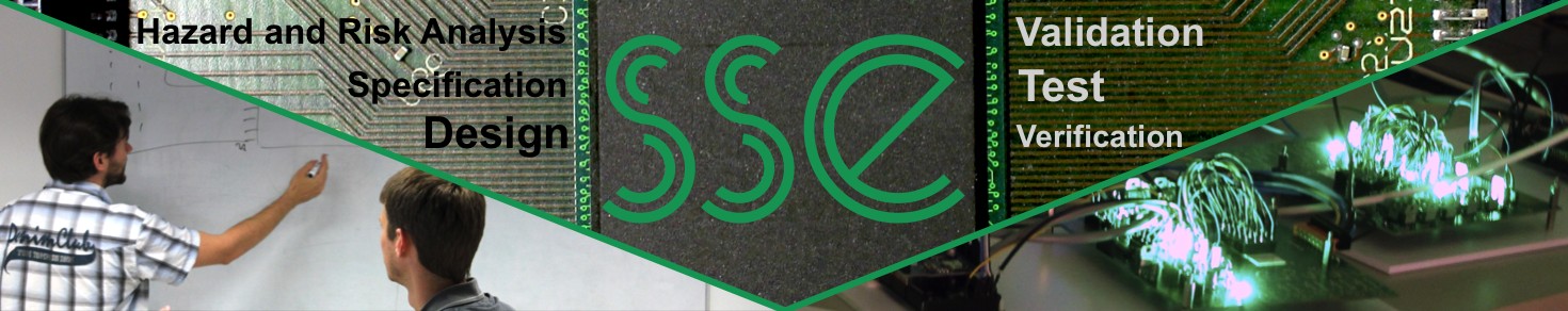
The course Hardware Acceleration Using FPGAs, consisting of a lecture and Practice session, takes place in winter semester and covers the practical use of commercial design tools. The practice covers complex design tasks based on the knowledge about design, modelling, description and synthesis of complex systems acquired from lectures of circuits and systems design and EDA-Tools with the help of further design tools. The lecture provides the necessary theoretical knowledge about tools and algorithm.
Lecture Timeline
Wednesday, odd week, 15.30 until 17.00 o'clock in room 2/W451.
L1 - Designflow
- Design phases
- System environment and testbenches
L2 - VHDL for FPGA (1)
- FPGA specific VHDL
- Design attributes for FPGA
- Reset and FSM treatment
L3 - VHDL for FPGA (2)
- Macros: RAM, ROM, GSR-Block
- Tips and Tricks
L4 - Synthesis for hierarchic systems
- Partitioning and Validation
- Constraints and specific scripts
L5 - XILINX ISE Foundation
- Design Flow
- Introduction into P&R tools, analysis of the generated reports
L6 - Timing analyse and Backannotation
- Timing information during design flow
- Backannotation simulation
L7+L8+IS - Working on complex design tasks + Special strategies for big hierarchic Systems + Intermediate Seminar
- L7: Teamwork, Project consistency
- L7: Verification strategies
- L8: Time management
- L8: Constraint dependencies, special script constructs
- IS: Evaluation of the current project state
- IS: Analysis of mistakes and difficulties
Practice Timeline
Wednesday, even week, from 15:30 until 18:30 o'clock, room 2/W465.
P1 - Synthesis requirement VHDL on the example Design Analyzer
P2 - Introduction into the Tools
- Introduction of Precision Synthesis, ModelSim, and Xilinx P&R-Tools
- Synthesis required VHDL
- Design-Flow
- Script programming