Device Reliability
The Functionality of a semiconductor device is limited by many factors. In the course of reliability investigations devices are being stressed cyclically under various ambient conditions and electrical conditioning within standardized tests or even further until failure. To reach sufficient comparability with other devices or test strategies, normalization and extensive statistical evaluations are inevitable.
HTGB - High Temperature Gate Bias Test
|
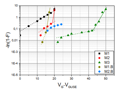
The gate oxide of voltage-controlled power semiconductors such as MOSFETs or IGBTs show a thickness around 100nm and can be even
smaller for silicon carbide-MOSFETs (SiC-MOSFETs). |

|
HTRB - High Temperature Reverse Bias Test
In HTRB tests (High Temperature Reverse Bias) power semiconductors are permanently exposed to a DC voltage to investigate the long-term stability of the blocking current. The high blocking voltage, usually at least 80% of the specified blocking voltage, together with a high junction temperature within 1000h simulates a life cycle of the test devices in the field. Weak points in the passivation layer or in the edge structure as well as on the chip edges can be detected. Mobile ions resulting from contamination during the manufacturing process can lead to localized field elevations and even accumulate to surface charges. Thus inversion channels can arise in low-doped areas and lead to an increase of the blocking current, which can short-circuit pn-junctions. To investigate this behavior a permanent measurement of the blocking current is required during the test.
H³TRB - High Humidity High Temperature Reverse Bias Test
In application areas such as photovoltaics or on- and offshore wind farms, power semiconductors are exposed to harsh environmental conditions. Particularly high humidity can damage the power switches by penetrating through the silicone soft encapsulant into modules and damaging the semiconductors through corrosion. The silicone used often has a high permeability, which absorbs moisture quickly but also releases it again quickly. In the H³TRB (High Humidity High Temperature Reverse Bias), a simultaneous exposure to high air humidity and high temperature under applied blocking voltage is simulated to investigate the influence on the blocking currents. The test takes place inside a climatic chamber under a temperature of 85°C at a relative humidity of RH=85%. The reverse voltage is limited to a maximum of 80V in most standards. The increasing technological progress in high-bandgap power semiconductors such as silicon carbide (SiC) and gallium nitride (GaN) has led to a modification of the test strategy. In HV-H³TRB tests, a reverse voltage of up to 80% of the specified blocking voltage can be applied to the test devices and thus further accelerate the aging process.
