Rolled-up Nanoelectronics
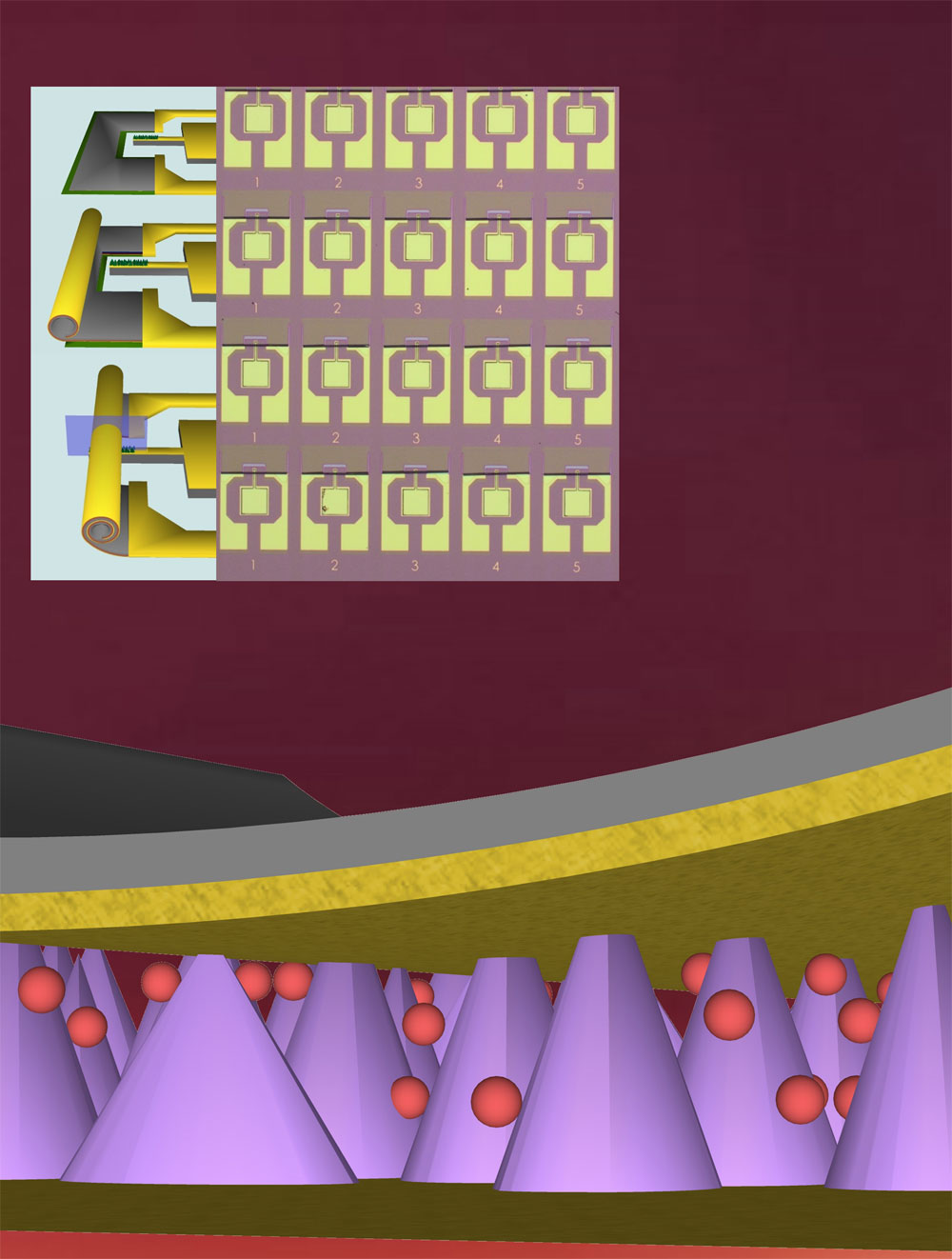
Fully integrated organic nanocrystal diode as high performance room temperature NO2 sensor
Full integration of nanoscale molecular structures with reliable electrical contacts has remained a persistent challenge in device fabrication procedures. In this work, by employing rolled-up technology we successfully create organic diodes consisting of molecular nano-pyramid structures sandwiched between metal and strained nanomembrane electrodes. The robust and smooth contacts provided by self-curled metal layers render the molecular nano-pyramids efficient channels for detecting nitrogen dioxide airflow. The devices demonstrate a high average sensitivity (151% ppm−1) and a fast recovery time (12 min) for NO2 detection.
Large-area rolled-up nanomembrane capacitor arrays
Miniaturization of electronic devices and reduction of their footprint areas are essential ingredients towards efficient development of energy autonomous systems and electronic circuitry. We demonstrate the feasibility of fabricating ultracompact energy storage elements employing rolled-up nanotechnology. These elements highlight the flexibility and high yield of the parallel fabrication process, which results in a substantial reduction in the device dimensions and better integration of the devices into future miniaturized electronic systems.
R. Sharma et al., Adv. Energy Mater. 4, 1301631 (2014), URL PDF

Thermal conductivity of mechanically joined semiconducting/metal nanomembrane superlattices
We fabricate in an unconventional but straight forward way hybrid superlattices consisting of a large number of nanomembranes mechanically stacked on top of each other. The superlattices can consist of an arbitrary composition of n- or p-type doped single-crystalline semiconductors and a polycrystalline metal layer. These hybrid multi-layered systems are fabricated by taking advantage of the self-rolling and pressed-back technique. The time-domain thermoreflectance measurements show a substantial reduction of the cross-sectional heat transport through the nanomembrane superlattice compared to a single nanomembrane layer below 2 W m-1K-1, which represents a reduction of two orders of magnitude compared to the respective bulk values. Scanning thermal atomic force microscopy measurements support the observation of reduced thermal transport on top of the superlattices with a spatial resolution of ~100nm. The low thermal conductivity reveals the potential of this approach to fabricate miniaturized on-chip solutions for energy harvesters in e.g. micro-autonomous systems.
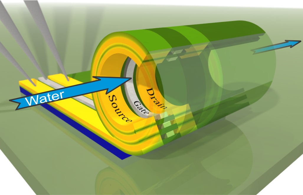
Rolled-up nanomembranes as compact 3D architectures for field effect transistors and fluidic sensing applications
We fabricate inorganic thin film transistors with bending radii of less than 5μm maintaining their high electronic performance with on-off ratios of more than 100000 and subthreshold swings of 160mV/dec. The fabrication technology relies on the roll-up of highly strained semiconducting nanomembranes, which compacts planar transistors into three-dimensional tubular architectures opening intriguing potential for microfluidic applications. Our technique probes the ultimate limit for the bending radius of high performance thin film transistors.

Animation of 3D rolled-up field effect transistor
D. Grimm
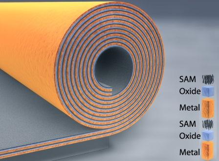
Self-wound ultra-compact energy storage elements
We have demonstrated the self-assembly of ultra-compact energy storage devices based on self-wound three-dimensional hybrid organic/inorganic nanomembranes. Such ultra-compact elements exhibit capacitances per footprint area higher than their state-of-the-art planar counterparts and reach specific energies comparable to supercapacitors. The combination of self-assembled organic monolayers with inorganic capacitor materials leads to elements with small footprints, remarkable performance and properties strongly correlated with the organic materials incorporated. Our results represent a breakthrough for local on-chip energy storage and energy supply for autonomous systems at the micro- and nanoscale.
C. C. Bof Bufon at al., Nano Lett. 10, 2506 (2010) URL PDF
This work was highlighted in:
- New Scientist Magazine (June 26, 2010) URL
- smartgrid (June 27, 2010) URL
- Pro-Physik.de (August 4, 2010) URL
- nanowerk (August 4, 2010) URL
- Scinexx (August 5, 2010) URL
- materialgates (August 6, 2010) URL
- electroniknet.de (August 12, 2010) URL
- GreenTech Germany (August 17, 2010) URL
- scienceknowledge.org (September 2, 2010) URL