Failure Analysis
In order to constantly advance the state of the art, it is necessary to know the weak points of current and older generations of power devices. Which fault patterns, are caused by which abnormal operating conditions and which wear marks occur under certain operating conditions? These and other questions require a comprehensive examination of the device, the package and the application.
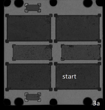
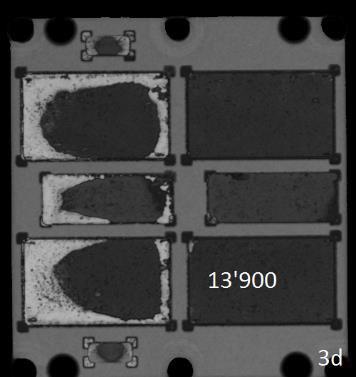
The object of the failure analysis is a comprehensive description of the current state of a power device and the traceability of failures or deteriorated operating conditions to the application. In addition to a visual inspection for mechanical damage, the investigations include an electrical function validation and finally a section-by-section analysis of the individual device layers.
|
|
Failure states and critically changed operating conditions of components can be attributed to various causes:
- Different thermal expansion coefficients within the power device and between the different layers of a power module
- Insufficient quality of the packaging process
- Unfavourably selected load profiles
- Critical switching and overload events
- ESD incidents and improper handling of power electronic assemblies
- Disregard of component critical environmental conditions
|
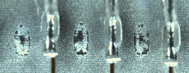
Ultimately, failure analysis, i.e. the assessment of the fault pattern and its cause, requires extensive examination of the device and the application on a mechanical, electrical and thermodynamic level. The analysis is supported by various methods:
- Optical and ultrasonic microscopy
- Bond wire pulling and shear tests
- Packaging and semiconductor simulation
- Power cycling and dynamic switching and overload tests
- Chemical preparation and removal of device layers