Successful Structure Search: Construction of Monoatomic Lead Layers with Specially Developed Method Unveiled for the First Time
Research team led by Chemnitz University of Technology synthesizes two-dimensional layer of lead using a novel method and describes its atomic structure in detail for the first time - Publication in renowned journal Advanced Materials Interfaces
-
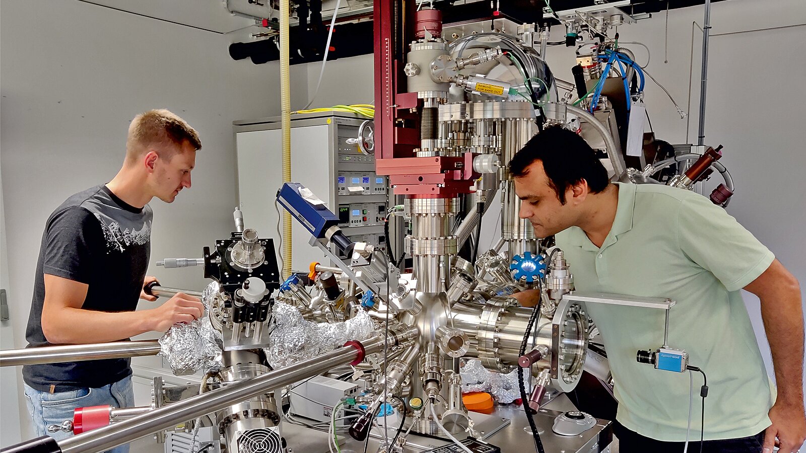
Chitran Ghosal (r.) and Dr Philip Schädlich examine the electronic properties of the 2D meat layers in a laboratory at the TUC's Institute of Physics. Photo: Franziska Schölzel
Scientists from the Professorship of Analysis of Solid Surfaces (Head: Prof. Dr. Christoph Tegenkamp) and the Professorship of Experimental Physics with a focus on Technical Physics (Head: Prof. Dr. Thomas Seyller) of Chemnitz University of Technology are researching the functionalization of low-dimensional electron gases as part of the research group "Proximity-induced correlation effects in low-dimensional structures (FOR 5242)".
In a recent publication in the renowned journal Advanced Materials Interfaces, the research team led by first author Dr. Philip Schädlich, a research associate at the Professorship of Experimental Physics with a focus on Technical Physics, presents a method for the detailed structural analysis of synthesized two-dimensional lead layers on a specially manufactured system for the first time. The presented approach has also made it possible to produce samples of sufficient quality to comprehensively describe the structures. The new insights from fundamental research could become relevant in the development of novel electronic systems and in the development of quantum materials for quantum computing.
"Our synthesis, together with a meticulous data analysis by the various groups, has now achieved this comprehensive picture of the two-dimensional lead layers," says Philip Schädlich. "The controlled coupling of functionalized graphene to 2D electron gases opens up the possibility to investigate and control correlation effects and mesoscopic phenomena in 2D materials - for example superconductivity, spin or charge density waves and novel magnetic phases," says Seyller.
To investigate these kinds of systems, the researchers, funded by the German Research Foundation (DFG), work across disciplines and locations. Partners from Jülich, Lund (Sweden), Hamburg, Regensburg, Göttingen, Stuttgart, and Braunschweig were involved. "The high degree of mixing with different professional competencies in our research group is necessary to be able to explore all facets of such complex problems in detail. Only in this way can structural and electronic properties of the self-made systems be linked," says Prof. Dr. Christoph Tegenkamp, spokesman for the DFG research group.
Trick of Nature: Domain Boundaries in Response to Unsaturated Bonds
"The structure formation of the 2D lead layer is based on motifs that we know from previous experiments on the adsorption of lead on silicon surfaces," explains Dr. Philip Schädlich, who coordinated most of the experiments. However, the flexibility of the lead bonds leads to a great variety in the phase diagram, for which the term "devil's staircase" has been established.
In contrast, in the current experiment, the lattice mismatch between the substrate and the lead layer results in a shortage of lead atoms per silicon atom of the substrate, resulting in strains in the lead and unsaturated bonds on the substrate surface.
The researchers now know why this is: "It's a trick of nature. The lead layer forms domains in which the lead atoms relax locally to their favorite distance and which are small enough so that the total offset between the lead and substrate lattice is not too large," Schädlich explains. "To do this, the centers of neighboring domains have to be slightly offset against each other, so that the resulting boundaries of the domains just contain enough lead atoms to automatically also compensate all unsaturated bonds," explains Chitran Ghosal, a doctoral student in Prof. Tegenkamp's working group.
Great Importance of Domain Boundaries
The structure of the lead layer also has an impact on the graphene. Because the evaluation of the data showed a vanishingly low charge carrier concentration, which is about 1000 times lower than in epitaxial graphene. "Unlike significantly more efficient intercalants such as hydrogen, the lead layer also manages to shield or compensate the spontaneous polarization of the substrate and thus provide for quasi-charge neutrality," Ghosal continues.
In addition, with the help of scanning tunneling microscopy at low temperatures of four Kelvin (approx. -269 degrees Celsius), the fingerprint of a so-called Kekulé ground state was revealed. Here too, the domain boundaries play a major role, as the electrons scattered on them, due to charge neutrality, only have a limited phase space available.
Background: DFG Research Group "Proximity-induced correlation effects in low-dimensional structures" led by Chemnitz University of Technology
Phenomena like the one currently described are at the heart of the DFG research group led by Prof. Tegenkamp. The research group, funded with over four million euros, has dedicated itself to investigating correlation effects in 2D materials and brings together the expertise of eight working groups from all over Germany. The goal is to manipulate 2D materials in a targeted manner and thus to research exotic effects such as superconductivity, charge density waves, Mott states, as well as the quantum Hall effect and Klein tunneling.
Publication: Philip Schädlich, Christoph Tegenkamp et al: Domain boundary formation within an intercalated Pb monolayer featuring charge-neutral epitaxial graphene, Adv. Mater. Interfaces (2023).
DOI: https://doi.org/10.1002/admi.202300471
For further information, please contact Prof. Dr. Tegenkamp, tel. +49 371 531-33103, e-mail christoph.tegenkamp@physik.tu-chemnitz.de, and Philip Schädlich, tel. +49 371 531-3170, e-mail philip.schaedlich@physik.tu-chemnitz.de.
(Author: Matthias Fejes / Translation: Brent Benofsky)
Matthias Fejes
24.07.2023