Technical Equipment
Microstructure analysis, material analysis and material characterization
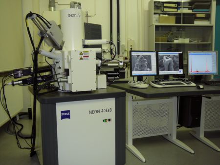
NEON40EsB field emission scanning electron microscope with EDXS and EBSD
- microscope
- Mapping of surface, ground or broken surfaces of:
- Starting materials (powders, fibers, foils)
- Materials, composite materials and composite materials
- coatings
- components
- Magnifications: 50x to 100,000x
- detectors:
- Chamber detector for secondary electrons
- Chamber detector for backscattered electrons
- Inlens detector for secondary electrons
- Inlens detector for backscattered electrons
- Light and dark field detector for transmitted electrons
- Energy dispersive X-ray microscope analysis (EDXS) EDAX Genesis
- Local chemical analysis on flat surfaces:
- for elements with order number Z ≥ 8
- Detection limit approx. 0.5% by weight for Z ≥ 11
- Quantification error approx. 2% by weight for main components
- Species:
- Average Analysis
- Phase analysis (for particle size > 1 μm)
- Element concentration distribution along a line (linescan)
- Two-dimensional element concentration distribution (mapping)
- Backscattered electron diffraction (EBSD) EDAX TSL
- Grain orientation analysis, orientation mapping, texture analysis
- Identification of crystalline phases, phase mapping
→ see also Analytical Scanning Electron Microscopy service
Contact Person

M. Sc. Andreas Gester
- Telefon:+49 371 531-33649
- Fax:+49 371 531- 833649
- Raum:3, 3/E001
- E-Mail: