Thermal Lab
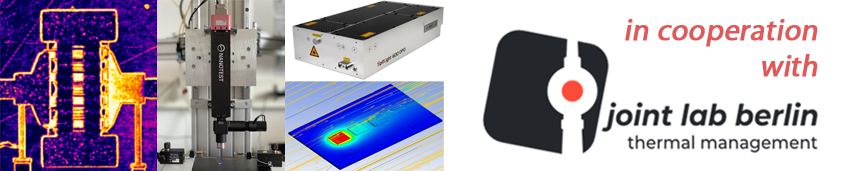
This lab is run in close cooperation with the Joint Lab Berlin
Thermo-reflectance (TR) Thermography
Features
- Thermal imaging on reflective surfaces
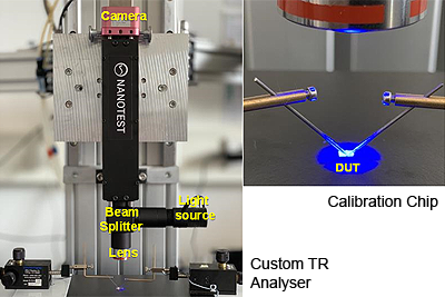
- Compact custom designed thermo-reflectance module
- Adjustable wavelength or white light
- Detection with CMOS sensor
- Higher resolution than mod-wave IR-imaging
Contact: Dr. Daniel May
Description
Compact and lightweight custom thermo-reflectance module. Temperature mapping on reflective surfaces with high lateral resolutions (down to 250 nm). System consists of sensitive CMOS detector with high full well capacity (200 ke-), low read out noise (3 e-) and high quantum efficiency >78%. Wide wavelength range from 460 nm - 780 nm, also broadband white light for multispectral illumination for measurements on typical materials used in electronics such as gold, aluminium, titanium, nickel, copper and chromium.
Typical Results
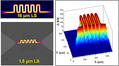
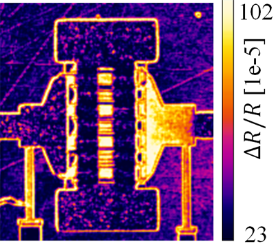
Thermal imaging on HEMT (high-electron-mobility transistor) device during operation. High power output of amplifier stage shows higher temperature (left side of HEMT). Resolution ≈ 500 nm higher than mid wave infrared imaging.
Thermal thin Layer Characterisation by Custom Laserflash
Features
- Determine thermal diffusivity and conductivity of thin layers
- Ultrashort optical laser pulse (∼7 ns)
- Tracking time of thermal pulse travelling through sample
- Wide range of specimens and parameters
Contact: Dr. Daniel May
Description
Thin layers can be subjected to an ultrashort optical pulse by a Laser to determine its thermal diffusivity and conductivity. The method tracks the time the thermal pulse needs to travel through the sample. The advantage is the universality of the setup which allows a wide range of specimens and parameters as e.g. geometry, temperature etc.. Thicknesses down to the µm-range can be characterised and accuracies to within ±5% can be obtained.
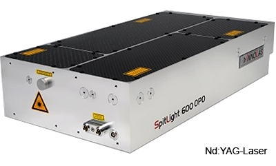
Laser SpitLight 600
- Wave length: 1064 nm, 532 nm
- Energy ∼800 mJ @ 1064 nm, ∼480 mJ @ 532 nm
- Pulse width ∼7 ns @ 10 Hz
- Beam Diameter 6 mm
- Special options: Energy Monitor, Pointing Laser
Typical Results
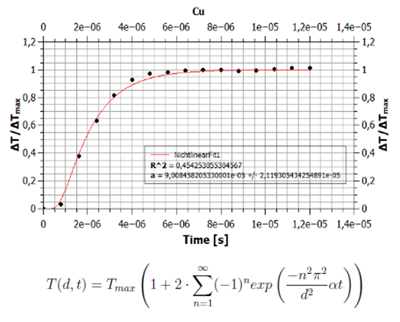
Typcal result for a thin Cu-membane. The measured data is fit by an analytical formula from which the diffusivity is obtained.
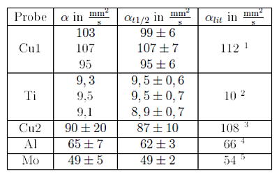
Very good agreement is reached upon comparison to literature values.