Jump to main content
Semiconductor Physics

Optical Spectroscopy

Members

  • Dr. Ovidiu D. Gordan
  • Stefan Moras (HiWi)
  • Oana-Maria Buja

Former Members:

  • Philipp Schäfer (PhD student), Li Ding (PhD student), Michael Ludemann (PhD student), Falko Seidel (PhD. student), Seddigeh Nikipar (PhD. student), Eric Schwuchow (Diploma student)

Topics

  • Complex Structures (QD structures, plasmonic nanostructures, metamaterials)
  • Oxides (high-k and wide bandgap materials)
  • 2D-Systems
  • Organic Semiconductors

Equipment

  • Ellipsometer: M-2000/T-Solar ( 0,7 - 5 eV), VASE  (0,7 - 5 eV), UVISEL HORIBA (1,5 - 6 eV) and RAS setups (home made; 1,5 - 5,5 eV)
  • FTIR: Vacuum spectrometer BRUKER VERTEX 80v and BRUKER IFS 66
  • Micro-Raman spectroscopy and imaging; excitation wavelengths from red to UV, under temperature and atmosphere controlled conditions
  • Raman: Dilor XY triple monochromator Raman system and LabRam HR800 confocal micro Raman system
  • Cryo stages

Examples


Figure 1: Scanning electron microscopy image of Ag nanostructures on a silicon substrate. 450 nm particles were used as a deposition mask. Nanosphere lithography is a versatile tool to fabricate plasmonic structures. The picture shows a scanning electron microscopy image of the resulting nanostructures. These nanostructures show a strong plasmonic effect. 

Figure 2: Ellipsometric Delta contrast image of periodic Au nanostructures on Si substrate recorded with an Accurion EP3-SE imaging ellipsometer (image courtesy of C. Röling, Accurion GmbH). The inset shows a typical SEM image of 400 nm2 of an Au array with a 130 nm period. On the left side the effective and modeled extinction coefficient for the region 6 are plotted.


Figure 3: Schematic drawing of the combination of the Dilor XY 800 Raman Spectrometer with an UHV chamber. This offers the opportunity to acquire Raman spectra during evaporation or during high temperature treatment under ultra-high vacuum conditions.

Publications

P. Tonndorf, R. Schmidt, P. Böttger, X. Zhang, J. Börner, A. Liebig, M. Albrecht, C. Kloc, O. Gordan, D.R.T. Zahn, S. Michaelis de Vasconellos, R. Bratschitsch
Optics Express 21, (4) (2013), 4908
Photoluminescence Emission and Raman Response of Monolayer MoS2, MoSe2, and WSe2

T. Ebert, G. Cox, E. Sheremet, O. Gordan, D.R.T. Zahn, F. Simon, S. Spange
Chem. Commun., 48 (2012), 8967
Carbon/Carbon Nanocomposites Fabricated by Base Catalyzed Twin Polymerization of Si-Spiro Compound on Graphite Sheets

R.D. Rodriguez, E. Sheremet, D.J. Thurmer, D. Lehmann, O. Gordan, F. Seidel, A.G. Milekhin, O. Schmidt, M. Hietschold, D.R.T. Zahn
Nanoscale Res. Lett., 7 (2012), 594
Temperature-dependent Raman Investigation of rolled up InGaAs/GaAs Microtubes

F. Haidu, O. Gordan, D.R.T. Zahn
Thin Solid Films, 520 (13) (2012), 4410
In situ Ellipsometric Study of Copper Growth on Silicon

F. Seidel, L. Ding, O. Gordan, D.R.T. Zahn
J. Vac. Sci. Technol. B, 30 (1) (2012), 012401-1
Multi-Phase Model for Reflection Anisotropy Spectra of Copper Phthalocyanine Films on Anisotropic Silicon Substrates

M. Ludemann, Iulia E. Brumboiu, O. Gordan, D.R.T Zahn
J. Nanoparticle Research, 13 (2011), 5855
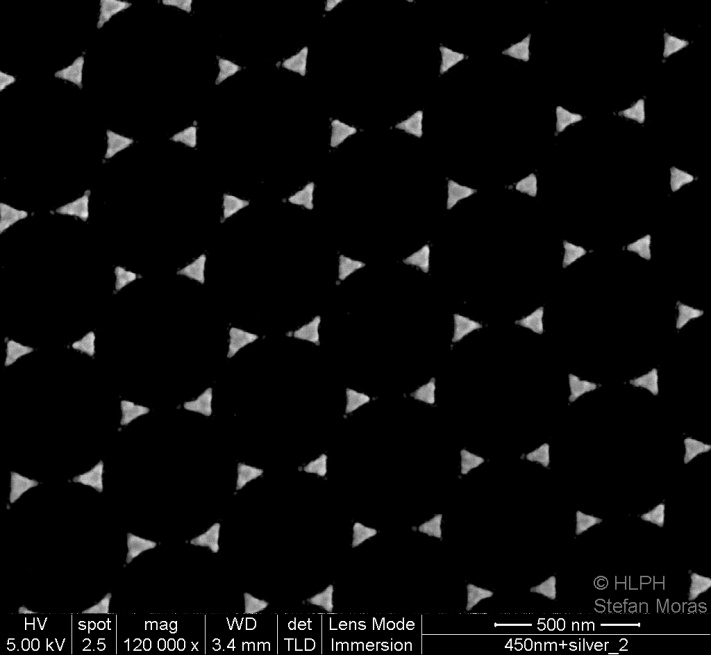
Surface-enhanced Raman Effect in Ultra-Thin CuPc Films Employing Periodic Silver Nanostructures

F. Haidu, M. Fronk, O. Gordan, G. Salvan, D.R.T. Zahn
Phys. Rev. B, 84 (2011), 195203-1
Dielectric Function and Magneto-optical Voigt Constant of Cu2O: A Combined Spectroscopic Ellipsometry and Polar MOKE Spectroscopy Study