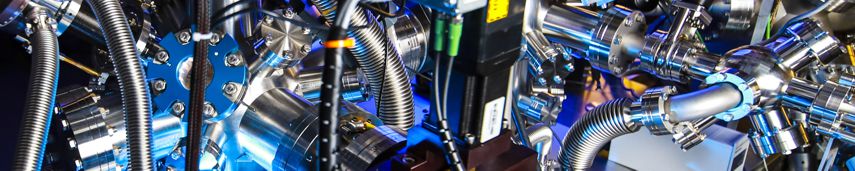
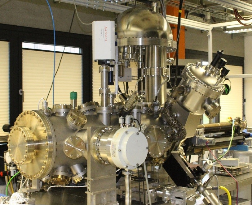
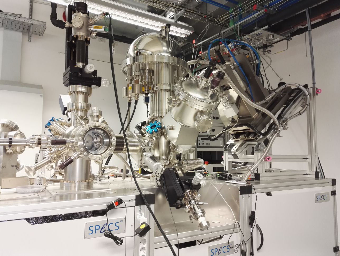
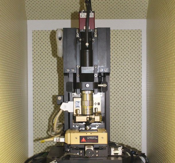
Spectrometer for X-ray photoelectron spectroscopy (XPS)
Ultrahigh vacuum chamber with
- Photoelectron analyzer (Specs Phoibos 150 with 9 channeltrons)
- Monochromated X-ray source (Specs Focus 500) for Al Kalpha and Ag Lalpha
- Electron flood gun for charge compensation
- Sample manipulator with heater up to 1200 °C
- Ar-Ion source (sputter gun)
- LEED optics
- Ports for evaporators, quartz crystal balance, mass spectrometer, etc.
Typical applications:
- Analysis of chemical composition of solids, thin films and surfaces
- Analysis if interfaces between thin films and substrates
- Electronic and structural properties of surfaces
|
 |
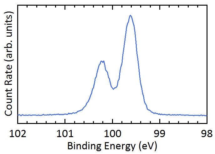
Si2p spectrum of a H-terminated Si(111) surface. |
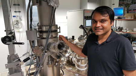
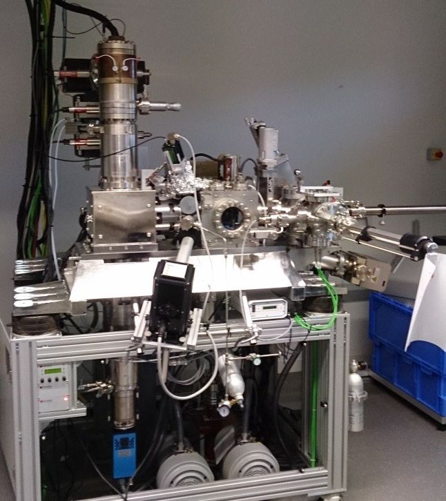
Spectrometer for angle-resolved photoelectron spectroscopy (ARPES)
Ultrahigh vacuum system including an analysis chamber with
- Photoelectron analyzer (Specs Phoibos 150 with 2D-CCD-Detektor)
- Monochromated X-ray source (Specs Focus 500) for Al Kalpha and Ag Lalpha
- UV source (Specs UVS 300) with monochromator (Specs TMM 304) for linear polarised HeI- und HeII-Radiation, polarisation rotatable by 90°
- 5-axis sample manipulator with liquid He cooling down to ca. 20 K
and a preparation chamber with
- Sample manipulator with heater uo to ca. 1000 °C und liquid N2 cooling to ca. 100 K
- Ar-Ion source (sputter gun)
- LEED optics
- Ports for evaporators, etc.
Typ. application:
- Band structure of solids and surfaces
- Analysis of chemical composition of solids, thin films and surfaces
- Analysis if interfaces between thin films and substrates
- Electronic and structural properties of surfaces
|
 |
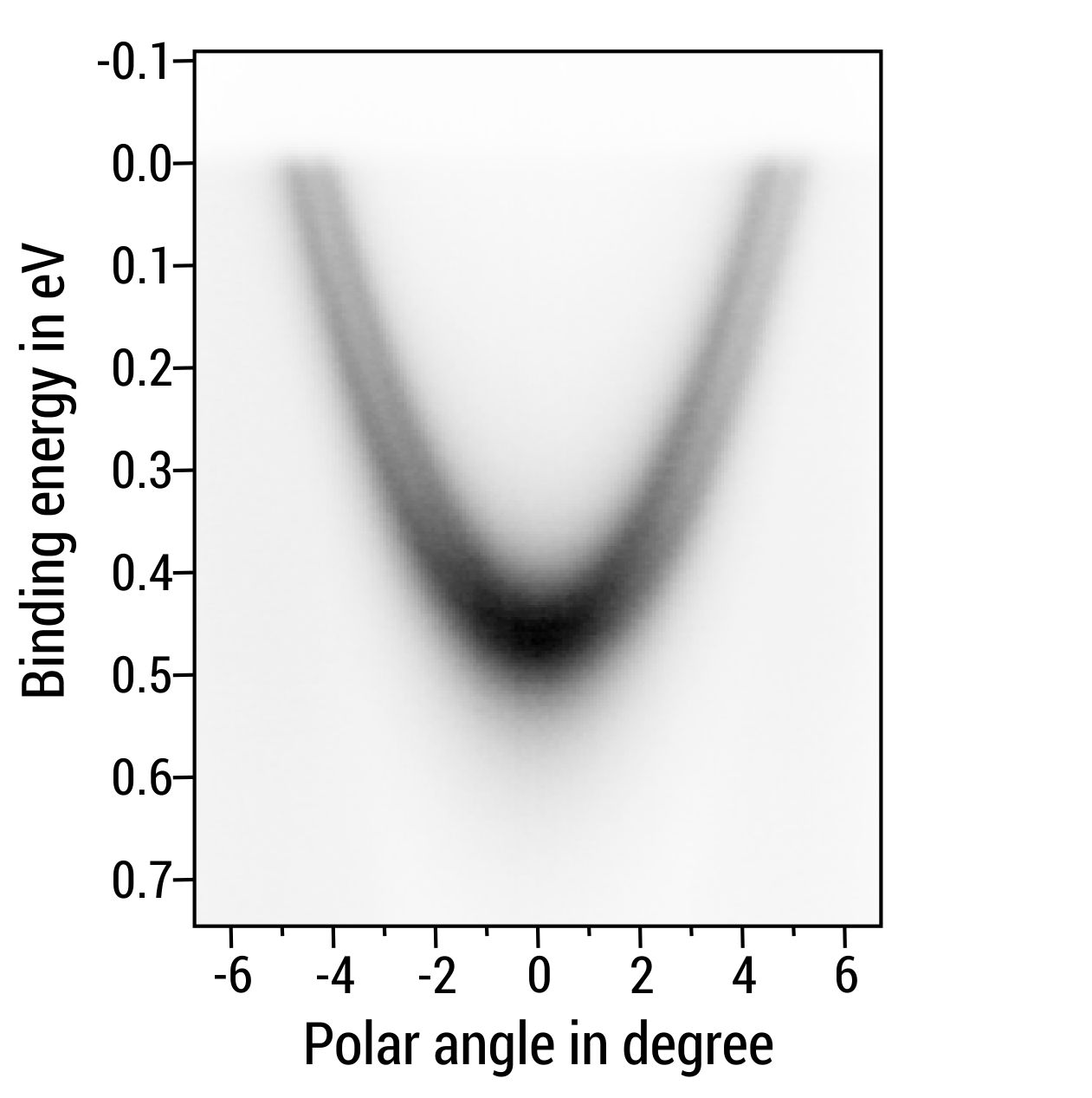
Surface state of Au(111). The Rashba splitting is clearly resolved.
(Monochrom. HeI, Epass =5 eV, Tsample=20K) |
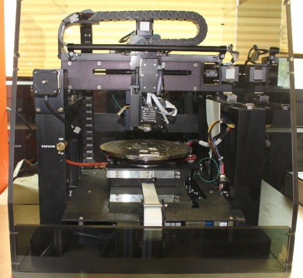
Low-energy electron microscope (LEEM)
System including an analysis chamber with
- Low-energy electron microscope (Specs FE-LEEM P90)
- Hg lamp für PEEM
- UV source für PEEM
- Sample heating up to ca. 1100 °C
and a preparation chamber with
- Ar-Ion source (sputter gun)
- Sample heating up to ca. 1100 °C
Typ. applications:
- Studies of thin film growth
- Structural and electronic proerties of surfaces and thin films
|
 |
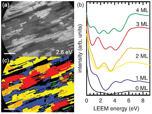
(a) LEEM bright filed image (ELEEM = 2.6 eV) of graphene on 4H-SiC(1-100). (b) Typical reflectivity spectra of areas with different thickness. (c) Fals solor image indicating the thickness distribution. From M. Ostler et al., Phys. Rev. B 88 (2013) 085408. |
Atomic force microscope (AFM)
System including
- Atomic force microscope (Park Systems XE100) under ambient conditions with optical mikroscope, motorized sample stage and separate z- and x/y-scanners
- Scanner for max. 5x5 µm2 and max. 100x100 µm2 scan areas
- Acousting enclosure
- Active damping of vibrations (Accurion)
Typ. applications:
- Investigation of structure und morphology of surfaces and thin films
|
 |
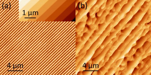
AFM images of a 6H-SiC(0001) surface after hydrogen etching (a) and after subsequent growth of graphene (b). |
Profilometer
- Stylus profilometer VEECO Dektak 8
Typ. applications:
- 2D und 3D maping of surface topographies of samples with up to 200 mm diameter
- Determination of thin film thickness and deposition rates.
|
 |
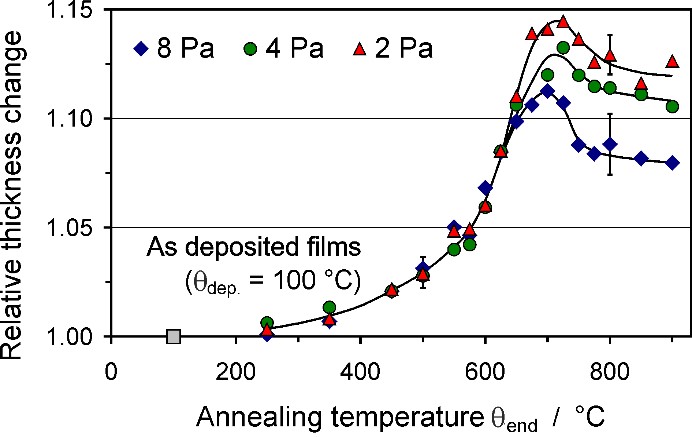
Increase of the thickness of a-C:H films deposited at 2 Pa to 8 Pa with the annealing temperature. From S. Peter et al., Diamond and Relat. Mater. 45 (2014) 43. |