Spintronic magnetic field sensing
Background
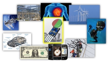
Magnetic field sensors have become omnipresent in everyday life. Their fields of application extend, just to name a few, from the automotive sector, to smart grid control and beyond to medical devices. They have literally become indispensable in a vast variety of technological scenarios as they enable contactless, precise and reliable measurements, even under tough operating conditions such as hot oil baths or exotic atmospheres. Free of wear and thus maintenance-free, they serve, for instance, as position and speed sensors not only in high-technology spacecraft rovers on Mars, but also in every modern automobile.
Since the technological breakthrough of spintronic magnetoresistive sensors on the basis of the giant magnetoresistive (GMR) effect in the last decade, and of the tunnel magnetoresistance (TMR) only a few years ago, entirely new perspectives are becoming reality. Compared to the established technologies of the Hall effect and anisotropic magnetoresistance (AMR), the nanoscale technologies GMR and TMR offer significantly improved signal levels at very fast response times in combination with an unprecedented degree of miniaturizability and low power consumption. The full biocompatibility of the GMR/TMR sensor technology along with its high miniaturizability allows, e.g., its employment for specific gen-antigen detection in lab-on-a-chip devices, as well as matrix-based non-invasive monitoring of cerebral and cardiac signals or smooth gastrointestinal examinations. Last but not least, magnetic field sensors have recently entered the market of mobile communication as their increasingly high sensitivity allows smart phone navigation based on the natural geomagnetic field.
 |
| Omnipresent magnetic field sensing |
Our current research and development on GMR and TMR sensors
Structures:
- GMR spin valves, GMR multilayers, magnetic tunnel junctions (TMR)
- in- and out-of-plane magnetic sensitivity
- Monolithic integration of 2D and 3D sensitivities in full-bridge configuration
Technology:
- PVD of metallic nanolayers for spintronic devices on wafer level
- Geometric sensor patterning techniques on wafer level, including (reactive) ion etching, electron beam etching, laser-based patterning*
- Microscopically resolved magnetic patterning on wafer level by means of laser-based heating and in-field cooling*
Applications:
- Fast microscopic electronic 2D/3D compass chip, e.g. for MEMS navigation in geomagnetic field
- Magnetic field visualization ("XMR magnetic field camera")
- Micro-magnetofluidic lab-on-a-chip applications for biomedical essays (specific electronic gen-antigen response, macromolecule and particle sorting and detection ...)
- ...
(* with partner Hochschule Mittweida)
 |
| Monolithic 2D GMR spin valve sensor in full-bridge configuration with microscopic magnetic pattern (schematic yellow arrows), direct response to rotation in geomagnetic field |
ContactProf. Dr. Stefan E. Schulz |
 Magnetic field sensor group in May 2014 |


