Thermoelectric materials
Thermoelectricity describes the interaction between thermal and electrical properties of a material. Well known are two main effects: the Seebeck effect (a temperature gradient in a material generates a thermal voltage) and the Peltier effect (a current in a material causes a heat flow in parallel, Fig. 1). These two effects lead to the main applications, as generator of electric energy and as cooling device. Especially for space missions thermoelectric energy generation is essential. Furthermore, the field of thermoelectricity is particularly in the focus of current research activities, since energy efficiency is becoming more and more important. However for the use in the field of energy conversation and for commercial applications the efficiency of the known thermoelectric materials is too small and therefore it is necessary to intensify the research in this area.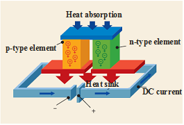 |  | ||
| Fig. 1 Principle of a Peltier element: On the upper side heat is absorbed and at the bottom released again [1]. | Fig. 2 Cassini probe: the energy was generated by thermoelectric materials [1]. |
Thermoelectric efficiency
Good thermoelectric materials are characterised by a high electrical conductivity σ, a large Seebeck coefficient S und a low thermal conductivity λ. These three properties are embodied in the so-called figure-of-merit Z: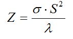
The Seebeck coefficient S is a material parameter and distinguishes the magnitude of the generated thermo voltage in a material with temperature gradient. A high electrical conductivity is necessary to minimize Joule heating, whilst a low thermal conductivity helps to retain heat at the junctions and maintain a large temperature gradient. Additionally the thermal conductivity can be split in an electronic (λel) and a phononic (λph) part. If Z is multiplied by the temperature, at which the material should be characterized, one gets the dimensionless figure of merit ZT. ZT is used to characterize thermoelectric materials and connected with the thermoelectric efficiency of the material:
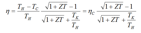
where ηC is the Carnot efficiency, TC the cold and TH the hot temperature at the end of the sample. This relation is shown in Fig. 3. By applying a temperature gradient of 500K, ZT-values of two or three are necessary to reach an efficiency of 20%. This efficiency is needed to use thermoelectric materials in commercial applications. The material group reaching the highest ZT values are semiconductors. Highly doped Bi2Te3 or SiGe were the most common thermoelectric materials in the past. An overview of the different material groups and their material coefficients is shown in Fig. 4. But even the established bulk materials (like Bi2Te3 oder SiGe) reach only a ZT value of 1. An further increase of ZT is difficult, because all electronic transport coefficients are linked to each other. One example is the Wiedemann-Franz-law, which connects λel and σ linearly.
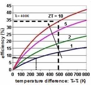 |  | ||
| Fig. 3 Relation between ZT and efficiency of thermoelectric materials [2]. | Fig. 4 Material Groups and their transport coefficient [1]. |
Thermoelectric Research
Nanostructured Thermoelectric Materials
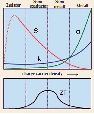
On possibility to decouple the transport coefficients is to go to low dimensional thermoelectric materials: thin films, multilayers (2D), nanotubes (1D) or nanoparticle (0D), Fig. 5,6. Here the electrical conductivity and/or the Seebeck coefficient could be increased due to an higher charge carrier density.Another method is to reduce the phononic part of the thermal conductivity by phonon scattering at grains, interfaces and defects. For example nanoparticles are pressed to nanocomposites to raise the amount of interfaces, at which the phonons are scattered. The phononic thermal conductivity can be reduced by epitaxial multilayers with conductance in cross plane direction too. While the electrical properties stay constant the phonons are scattered at the interfaces between the layers.
Additionally, combinations of all these approaches are possible, e.g. quantum dot multi layers, superlattice structures, multilayer nanotubes.
 | 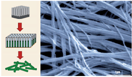 | ||
| Fig. 5 Multilayer structures; in plane: higher electric conductivity by reducing dimensions; cross plane: phonon scattering at the interfaces [1]. | Fig. 6 Thermoelectric nanotubes: by reducing to two dimensions electrical conductivity is increased [1]. |
Novel materials
An example for a modern thermoelectric material is the skutterudite CoSb3. CoSb3 is a semiconductor and has in general good thermoelectric properties. It belongs to the group of Phonon glass electron crystals (PGEC) with big voids in the their atomic structure (Fig. 7). These voids can be filled with loose bounded guest ions. Because of this weak bounding the ions are able to oscillate ("rattle") very strong and phonons are effectively scattered. This results in a reduced thermal conductivity and much better thermoelectric properties. Possible filling ions are for example rare earths metals, alkali earth metals, Ytterbium and Thallium. Many interesting properties of filled CoSb3 depend strongly on the filling ion, e.g. ferromagnetism, superconductance, spin polarisation. With this special properties filled CoSb3 is a promising candidate for future thermoelectric applications.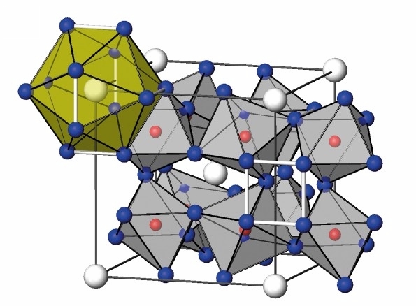 | |
| Fig. 7 Schematic illustration of the skutterudite structure; red: Co atoms, blue: Sb atoms, white: guest Ions; the big voids (yellow shaded) are filled with guest ions, which scatter phonons effectively [3]. |
Our research activities
We are investigating thin films of Co-Sb alloys. These films are prepared by molecular beam epitaxy. Therefore cobalt is evaporated with an electron gun and antimony with an effusion cell. To deposit films with different thickness and composition, the Co rate is controlled by an optical measurement system while the Sb rate is kept constant. Additionally the substrate temperature during the deposition can be changed.After the deposition, growth and structure of the films are investigated as function of composition, substrate temperature, and film thickness with the following methods:
- AFM to get information about the surface structure of the films (Fig. 8)
- RBS to achieve composition and thickness of the films
- XRD to investigate the crystal structure, the included phases and the lattice parameter
- AES to investigate composition ratios at the surface
- four probe resistivity measurements to determine the electrical conductivity at room temperature
- and a cryostat with Van-der-Pauw measurement system to investigate the conductivity in a temperature range between 4K and 300K.
 | |
| Fig. 8 AFM images showing the surface of CoSb3-layers |
[2] D. M. Rowe and C. M. Bhandari, Modern Thermoelectrics, 1983
[3] A. Leithe-Jasper and W. Schnelle. Gefüllte Skutterudite, Tätigkeitsbericht 2006 MPI Dresden